|
No. |
Item |
Standard Specification |
||
|
Formula |
Purity |
Impurity PPM Max each |
||
|
1 |
Cadmium Arsenide |
Cd3As2 |
4N 5N |
Available Upon Request. Special specification can be customized |
|
2 |
Gallium Arsenide |
GaAs |
5N 6N 7N |
|
|
3 |
Niobium Arsenide |
NbAs |
3N5 |
|
|
4 |
Indium Arsenide |
InAs |
4N 5N 6N |
|
|
5 |
Size |
-60/-80mesh, 1-20mm Lump, 1-6mm Granule, Target or Blank | ||
|
6 |
Packing |
In polyethylene bottle or composite bag, 1kg each. |
||
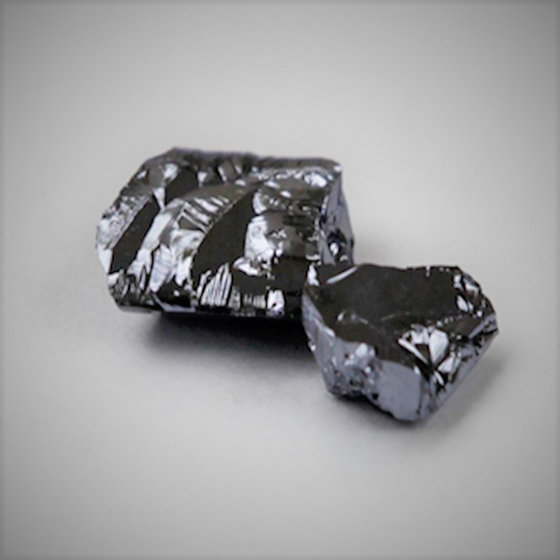
Niobium Arsenide Nb5As3 or NbAs, off-white crystalline solid, CAS No.12255-08-2, formula weight 653.327 Nb5As3 and 167.828 NbAs, is a binary compound of Niobium and Arsenic with the composition NbAs,Nb5As3, NbAs4 …etc synthesized by CVD method, these solid salts have very high lattice energies and are toxic due to the inherent toxicity of arsenic. High temperature thermal analysis shows NdAs exhibited arsenic volatilization upon heating. Niobium Arsenide Nb5As3 99.99% powder or lump is a crystalline solid in applications for semiconductor, photo optic, laser light-emitting diodes, quantum dots, optical and pressure sensors, as intermediates, and to fabricate superconductor etc. It should be kept in a well-closed, light-resistant, dry and cool place.
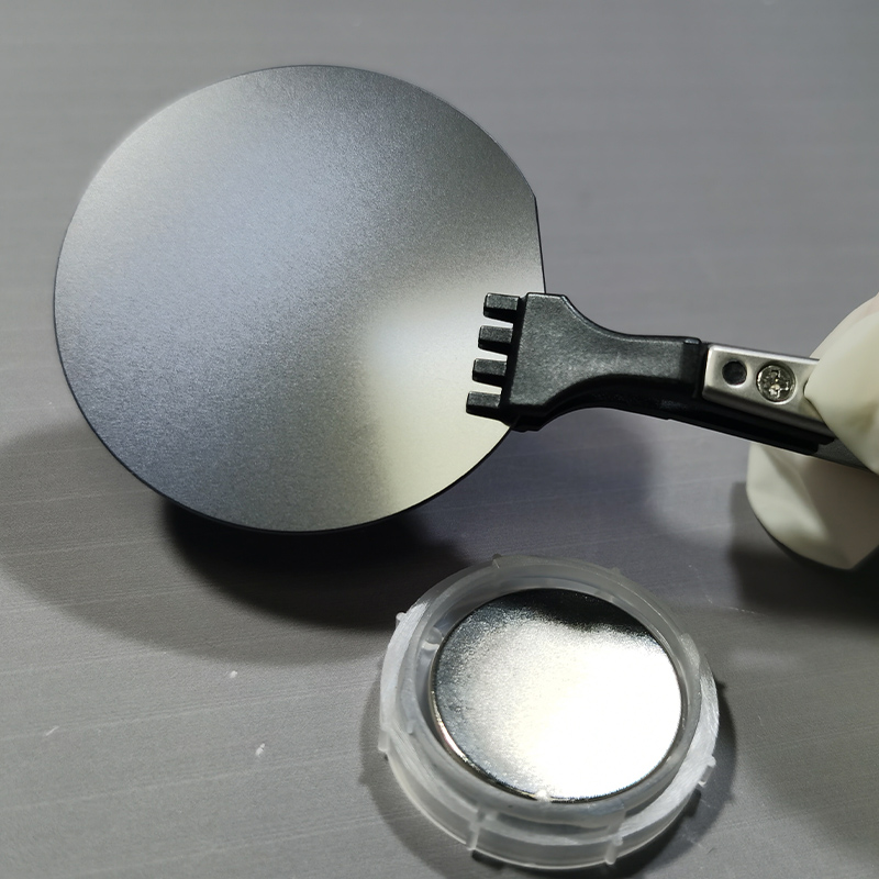
Gallium Arsenide GaAs, a III–V compound direct-gap semiconductor material with a zinc blende crystal structure, is synthesized by high purity gallium and arsenic elements, and can be sliced and fabricated into wafer and blank from single crystalline ingot grown by Vertical Gradient Freeze (VGF) method. Thanks to its saturating hall mobility and high power & temperature stability, those RF components, microwave ICs & LED devices made by it all achieve great performance in their high frequency communication scenes. Meanwhile, its UV light transmission efficiency also allows it to be a proven basic material in Photovoltaic industry. Gallium Arsenide GaAs wafer up to 6"(150mm) can be supplied, and 6N 7N and mechanical grade are available. Meanwhile, the polycrystalline Gallium Arsenide bar and lump are also customized upon request.
Indium Arsenide InAs, a direct-band-gap semiconductor crystallizing in the zinc-blende structure, compound by high purity indium and arsenic elements, grown by Liquid Encapsulated Czochralski (LEC) method, can be sliced into and fabricated into wafer from single crystalline ingot. Due to the low dislocation density but constant lattice, InAs is an ideal substrate to further support the heterogeneous InAsSb, InAsPSb & InNAsSb structures, or AlGaSb superlattice structure. Therefore, it plays an important role in 2-14 μm wave range infrared emitting devices fabrication. Besides, the supreme hall mobility but narrow energy bandgap of InAs also allows it to become the great substrate for hall components or other laser & radiation devices manufacturing. Indium Arsenide InAs wafer of 2" 3" 4" is available. Meanwhile, the polycrystalline Indium Arsenide lump is also customized upon request.