|
No. |
Item |
Standard Specification |
||
|
Formula |
Purity |
Impurity PPM Max each |
||
|
1 |
Antimony Selenide |
Sb2Se3 |
4N 5N |
Available Upon Request. Special specification can be customized |
|
2 |
Arsenic Selenide |
As2Se3 |
4N 5N |
|
|
3 |
Bismuth Selenide |
Bi2Se3 |
4N 5N |
|
|
4 |
Cadmium Selenide |
CdSe |
4N 5N 6N |
|
|
5 |
Copper Selenide |
CuSe |
4N 5N |
|
|
6 |
Gallium Selenide |
Ga2Se3 |
4N 5N |
|
|
7 |
Indium Selenide |
In2Se3 |
4N 5N |
|
|
8 |
Lead Selenide |
PbSe |
4N |
|
| 9 | Molybdenum Selenide |
MoSe2 |
4N 5N |
|
|
10 |
Tin Selenide |
SnSe |
4N 5N |
|
|
11 |
Tungsten Selenide |
WSe2 |
3N 4N |
|
|
12 |
Zinc Selenide |
ZnSe |
4N 5N |
|
|
13 |
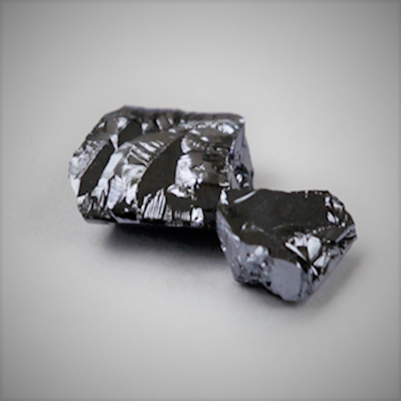
Size |
-60/-80mesh, 1-20mm Lump, 1-6mm Granule, Target or Blank |
||
|
14 |
Packing |
In polyethylene bottle or composite bag, 1kg each. |
||
Cadmium Selenide CdSe, purity 99.999% in form of powder or granule, most common Wurtzite hexagonal and red to black crystal, CAS 1306-24-7 atomic weight 191.377, density 5.8g/cm3, melting point 13500C, insoluble in Water is a solid, binary primarily ionic compound of cadmium and selenium. Polycrystalline compounds is synthesized by the High-Pressure Vertical Bridgman method or High-Pressure Vertical Zone Melting, or distillation and CVD synthesis, which is used for growing CdSe single crystal, CdSe evaporation material, namely for making photocell, rectifier, luminous paint, etc. Cadmium selenide with wurtzite crystal structure is an important II-VI n-type semiconductor, and has a band gap of 1.74 eV. CdSe nanoparticle by several production methods of arrested precipitation in solution, synthesis in structured media, high temperature pyrolysis, sonochemical, and radiolytic methods is of 1–100 nm in size, exhibits a property known as quantum confinement, they are finding applications in opto-electronic devices such as laser diodes that cover a large part of the electromagnetic spectrum, especially useful as a component of photocatalysts, use in biomedical imaging applications, and is used in windows for instruments using infra-red (IR) light, nanosensing and high-efficiency solar cells.
Copper Selenide or Dicopper Selenide, Cuprous Selenide, CAS No 20405-64-5, black cubic crystal, is 99.999% 99.9999% purity in form of ingot, powder, pill, granule or needle etc, density 6.749, melting point 11130C, insoluble in water but easily soluble in nitric acid, soluble in sulfuric acid and ammonia. Copper Selenide is prepared in a vacuum quartz seal tube placed in horizontal synthesis furnace. Ligand-stabilized copper selenide (Cu(2-x)Se) nanocrystal is synthesized by a colloidal hot injection process, which readily disperse in water and exhibit strong near-infrared (NIR) optical absorption with a high molar extinction coefficient, it finds application in photothermal therapy, ad for the preparation of group compound semiconductor, cuprous selenide target material, copper-indium-gallium-Selenium CIGS thin film solar cell etc.
Tungsten Selenide or Tungsten Diselenide, WSe2 CAS 12067-46-8, density 9.32g/cc, molecular weight 341.76, insoluble in water, is 99.99% , 99.995% 4N 4N5 purity in form of black powder or lump. Tungten Diselenide belongs to group V transition metal dihaloalkanes TMDC. WSe2 is a P-type or N-type semiconductor with an indirect band gap of ~ 1.3ev, and a single layer of WSe2 has a direct band gap. These layers are stacked together by vander Waals interaction and can be stripped into thin 2D layers. Being Lamellar structured, dry and solid lubricant, WSe2 has the lowest thermal conductivity with exceptional stability at high temperatures and in high vacuum. Tungsten Selenide thin films for terrestrial photovoltaic is synthesized by Chemical-Vapor-Deposition CVD, which can be for flexible thin film solar cell, or as a puttering target.
Gallium Selenide or Gallium Triselenide Ga2Se3, CAS 12024-11-2, molecular mass148.68, melting point 960°C density 5.030g/cm3, a dark brown, shiny flake crystal with hexagonal structure; 99.999% 5N purity, is a compound of Gallium and Selenium by chemical vapor deposition CVD method. GaSe is a layered semiconductor belongs to the family of metal chalcogens that crystallize in a layered structure. With the decrease of temperature, the maximum value of photoelectric effect of GaSe moves to the direction of short wave. Gallium Selenide GaSe crystal can be synthesized through different growth techniques of Bridgman growth, chemical vapor transport CVT and flux zone growth to optimize grain sizes and reduce defect concentrations. Gallium selenide GaSe crystal is proposed as the active compound for use in photovoltaic devices suited towards electronic and optical applications in 2D materials field, as intercalation electrodes in electrochemical lithium cells, and as a nonlinear optical medium.
Indium Selenide, or Diinsium Triselenide In2Se3, black to dull grease luster powder or lump, CAS No 2056-07-4, melting point 6600C, density 5.55g/cm3, is a compound of indium and selenium with 99.999%, 99.9999% 5N 6N purity. It is stable under room temperature and pressure, and kept to avoid light, open fire and high temperature. It is soluble in strong acid and easy to decompose. The semiconductive compound In2Se3 has a defective ZnS lattice structure in which the non-metallic atoms are arranged in tetrahedron by three metal atoms and one vacancy. To ensure structural, optical, and electronic consistency, Indium Selenide or Diindium Triselenide InSe is developed by Brigmann method preferable to offer highly crystallization as well as large size. Besides, the Flux Zone Growth and Chemical Vapor Transport CVT growth techniques are also optional. In2Se3 crystal is a direct gap semiconductor of 1.56eV emission (300K), α- In2Se3 and β- In2Se3 crystals are the two most common forms with defect wurtzite structures. It is mainly used as semiconductor, optical materials, photovoltaic devices, electrical sensors, or to be used for preparing copper indium gallium selenium CIGS thin film material.